written by James YS Kim
javakys@gmail.com
When one try SPI communication on STM32 MCU, he faces its poor throughput. This is because there is too long of an idle time between SPI read/write operations
The below image has the real SPI signals which were captured during the standard SPI communication and you can see the idle time is over 5 times longer than the one byte data communication time.
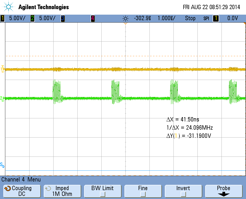
Figure1. SPI clock capture view in standard mode
STM32 MCU provides a method to enhance the SPI communication throughput by eliminating idle time between SPI read/write operations. It is SPI DMA mode.
Figure 2 shows that transmission and reception of block data is done continuously without any idle time when you use SPI DMA mode.
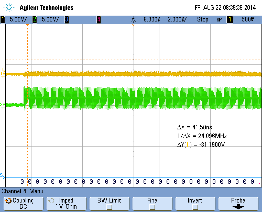
Figure2. SPI clock capture view in SPI DMA mode
I’ll show you how to enhance the SPI communication throughtput using SPI DMA mode in detail and in stage by stage.
SPI DMA mode
Not only STM32F2xx or STM32F4xx series but STM32F1xx series have been providing SPI DMA mode for bust data transmission. But there were some reports in which byte shift happens.
STM32F2xx and STM32F4xx series enhanced DMA mechanism to support stable, fast read/write operation.For details, refer to the application note, “AN4031: Using the STM32F2 and STM32F4 DMA controller”, from STMicro.
Using SPI DMA on STM32F401RE
Here, I’ll explain the way how to use SPI DMA step by step on STM32F401RE supporting the enhanced SPI DMA mechanism. Only system configuration part for using SPI DMA is included and refer to “Upgrade W5500 throughput on Nucleo STM32F401RE Using SPI DMA” for example.
SPI1 port selection
STM32F401RE supports up to 4 SPIs but SPI1 is selected for SPI communication.
DMA selection
Additional concepts like Channel and Stream are used in the enhanced DMA mechanism. The DMA Channel and Stream is decided upon which SPI peripheral is selected.
The above application note shows DMA request mapping table, refer to this table for selection of DMA Channel and Stream


Because SPI1 was selected for communication above, Channel3 of DMA2 was selected for SPI1_RX and SPI1_TX, Stream2 will be used for Rx and Stream3 for Tx.
Implementing code
1. RCC Clock Setting
Make the Peripheral clocks, RCC_AHB1Periph_DMA2 for DMA2 and RCC_APB2Periph_SPI1 for SPI1, ‘Enable’.
RCC_AHB1PeriphClockCmd( RCC_AHB1Periph_DMA2, ENABLE);
RCC_APB2PeriphClockCmd( RCC_APB2Periph_SPI1, ENABLE);
2. GPIO Setting
Set SCLK, MISO and MOSI pin of SPI peripheral to pull-down and map ‘Alternate Function’ to those pins.
GPIO_InitStructure.GPIO_OType = GPIO_OType_PP;
GPIO_InitStructure.GPIO_PuPd = GPIO_PuPd_DOWN;
GPIO_InitStructure.GPIO_Mode = GPIO_Mode_AF;
Set GPIO_AF_SPI1 as Alternate Function.
/* Connect SPI pins to AF_SPI1 */
GPIO_PinAFConfig(GPIOA, GPIO_PinSource5, GPIO_AF_SPI1); //SCLK
GPIO_PinAFConfig(GPIOA, GPIO_PinSource7, GPIO_AF_SPI1); //MOSI
GPIO_PinAFConfig(GPIOA, GPIO_PinSource6, GPIO_AF_SPI1); //MISO
This is the whole code for GPIO setting..
GPIO_InitStructure.GPIO_Pin = WIZ_SCLK | WIZ_MISO | WIZ_MOSI;
GPIO_InitStructure.GPIO_Mode = GPIO_Mode_AF;
GPIO_InitStructure.GPIO_Speed = GPIO_Speed_50MHz;
GPIO_InitStructure.GPIO_OType = GPIO_OType_PP;
GPIO_InitStructure.GPIO_PuPd = GPIO_PuPd_DOWN;
GPIO_Init(GPIOA, &GPIO_InitStructure);

GPIO_InitStructure.GPIO_Pin = WIZ_SCS | WIZ_nRST;
GPIO_InitStructure.GPIO_Mode = GPIO_Mode_OUT;
GPIO_InitStructure.GPIO_Speed = GPIO_Speed_50MHz;
GPIO_Init(GPIOA, &GPIO_InitStructure);
GPIO_SetBits(GPIOA, WIZ_SCS);
GPIO_SetBits(GPIOA, WIZ_nRST);

/* Connect SPI pins to AF_SPI1 */
GPIO_PinAFConfig(GPIOA, GPIO_PinSource5, GPIO_AF_SPI1); //SCLK
GPIO_PinAFConfig(GPIOA, GPIO_PinSource7, GPIO_AF_SPI1); //MOSI
GPIO_PinAFConfig(GPIOA, GPIO_PinSource6, GPIO_AF_SPI1); //MISO
3. SPI Setting
Set SPI Direction as FullDuplex and SPI Prescaler with SPI_BaudRatePrescaler_2 which is the fastest one.
SPI_InitTypeDef SPI_InitStructure;

/* SPI Config */
SPI_InitStructure.SPI_Direction = SPI_Direction_2Lines_FullDuplex;
SPI_InitStructure.SPI_Mode = SPI_Mode_Master;
SPI_InitStructure.SPI_DataSize = SPI_DataSize_8b;
SPI_InitStructure.SPI_CPOL = SPI_CPOL_Low;
SPI_InitStructure.SPI_CPHA = SPI_CPHA_1Edge;
SPI_InitStructure.SPI_NSS = SPI_NSS_Soft;
SPI_InitStructure.SPI_BaudRatePrescaler = SPI_BaudRatePrescaler_2;
SPI_InitStructure.SPI_FirstBit = SPI_FirstBit_MSB;
SPI_InitStructure.SPI_CRCPolynomial = 7;

SPI_Init(SPI1, &SPI_InitStructure);

while(SPI_I2S_GetFlagStatus(SPI1, SPI_I2S_FLAG_TXE) == RESET) ;
4. DMA Setting
If the length of data which you will read/write is fixed, then you can set its buffer size, the base address of buffer and so on at the initialization stage. Otherwise, you need to initialize them every time. So you’d better initialize DMA Stream only at the DMA initialization stage.
/* Deinitialize DMA Streams */
DMA_DeInit(DMA2_Stream3); //SPI1_TX_DMA_STREAM
DMA_DeInit(DMA2_Stream2); //SPI1_RX_DMA_STREAM
5. Implementing code for data communication
First, set data byte count to read/write by DMA.
DMA_InitStructure.DMA_BufferSize = (uint16_t)(tx_len + 3);
Second, initialize like below to process DMA by per byte.
DMA_InitStructure.DMA_FIFOMode = DMA_FIFOMode_Disable ;
DMA_InitStructure.DMA_FIFOThreshold = DMA_FIFOThreshold_1QuarterFull ;
DMA_InitStructure.DMA_MemoryBurst = DMA_MemoryBurst_Single ;
DMA_InitStructure.DMA_MemoryDataSize = DMA_MemoryDataSize_Byte;
DMA_InitStructure.DMA_MemoryInc = DMA_MemoryInc_Enable;
DMA_InitStructure.DMA_Mode = DMA_Mode_Normal;

DMA_InitStructure.DMA_PeripheralBaseAddr = (uint32_t)(&(SPI1->DR));
DMA_InitStructure.DMA_PeripheralBurst = DMA_PeripheralBurst_Single;
DMA_InitStructure.DMA_PeripheralDataSize = DMA_PeripheralDataSize_Byte;
DMA_InitStructure.DMA_MemoryDataSize = DMA_MemoryDataSize_Byte;
DMA_InitStructure.DMA_PeripheralInc = DMA_PeripheralInc_Disable;
DMA_InitStructure.DMA_Priority = DMA_Priority_High;
Third, Set DMA Channel3 and DMA2 Stream3 as DMA SPI Tx stream
Set DMA_DIR with DMA_DIR_MemoryToPeripheral because Tx stream sends data in DMA Memory to SPI1(Peripheral)
/* Configure Tx DMA */
DMA_InitStructure.DMA_Channel = DMA_Channel_3;
DMA_InitStructure.DMA_DIR = DMA_DIR_MemoryToPeripheral;
DMA_InitStructure.DMA_Memory0BaseAddr = (uint32_t) pTmpBuf1;
DMA_Init(DMA2_Stream3, &DMA_InitStructure);
Fourth, Set DMA Channel3 and DMA2 Stream2 as DMA SPI Rx stream.
In case of this Rx stream, set DMA_DIR with DMA_DIR_PeripheralToMemory.
/* Configure Rx DMA */
DMA_InitStructure.DMA_Channel = DMA_Channel_3;
DMA_InitStructure.DMA_DIR = DMA_DIR_PeripheralToMemory;
DMA_InitStructure.DMA_Memory0BaseAddr = (uint32_t) pTmpBuf1;
DMA_Init(DMA2_Stream2, &DMA_InitStructure);
Fifth, add code to control SPI Chip Select
wizchip_select();
…
wizchip_deselect();
Sixth, make DMA Stream enabled and SPI Rx/Tx DMA request enabled then SPI_Cmd enabled.
DMA_Cmd(DMA2_Stream3, ENABLE); /* Enable the DMA SPI TX Stream */
DMA_Cmd(DMA2_Stream2, ENABLE); /* Enable the DMA SPI RX Stream */

/* Enable the SPI Rx/Tx DMA request */
SPI_I2S_DMACmd(SPI1, SPI_I2S_DMAReq_Rx, ENABLE);
SPI_I2S_DMACmd(SPI1, SPI_I2S_DMAReq_Tx, ENABLE);

SPI_Cmd(SPI1, ENABLE);
Seventh, wait until SPI DMA operation finishes, and when done.
/* Waiting the end of Data transfer */
while (DMA_GetFlagStatus(DMA2_Stream3, DMA_FLAG_TCIF3)==RESET);
while (DMA_GetFlagStatus(DMA2_Stream2, DMA_FLAG_TCIF2)==RESET);
Eighth, deselect SPI Chip Select pin, clear DMA Flag, make DMA Stream disabled, make SPI Rx/Tx DMA request disabled and make SPI_Cmd disabled, then DMA transaction is over..
Below is the whole code for data communication using SPI DMA mode.
DMA_InitStructure.DMA_BufferSize = (uint16_t)(tx_len + 3);
DMA_InitStructure.DMA_FIFOMode = DMA_FIFOMode_Disable ;
DMA_InitStructure.DMA_FIFOThreshold = DMA_FIFOThreshold_1QuarterFull ;
DMA_InitStructure.DMA_MemoryBurst = DMA_MemoryBurst_Single ;
DMA_InitStructure.DMA_MemoryDataSize = DMA_MemoryDataSize_Byte;
DMA_InitStructure.DMA_MemoryInc = DMA_MemoryInc_Enable;
DMA_InitStructure.DMA_Mode = DMA_Mode_Normal;

DMA_InitStructure.DMA_PeripheralBaseAddr = (uint32_t)(&(SPI1->DR));
DMA_InitStructure.DMA_PeripheralBurst = DMA_PeripheralBurst_Single;
DMA_InitStructure.DMA_PeripheralDataSize = DMA_PeripheralDataSize_Byte;
DMA_InitStructure.DMA_MemoryDataSize = DMA_MemoryDataSize_Byte;
DMA_InitStructure.DMA_PeripheralInc = DMA_PeripheralInc_Disable;
DMA_InitStructure.DMA_Priority = DMA_Priority_High;

/* Configure Tx DMA */
DMA_InitStructure.DMA_Channel = DMA_Channel_3;
DMA_InitStructure.DMA_DIR = DMA_DIR_MemoryToPeripheral;
DMA_InitStructure.DMA_Memory0BaseAddr = (uint32_t) pTmpBuf1;
DMA_Init(DMA2_Stream3, &DMA_InitStructure);

/* Configure Rx DMA */
DMA_InitStructure.DMA_Channel = DMA_Channel_3;
DMA_InitStructure.DMA_DIR = DMA_DIR_PeripheralToMemory;
DMA_InitStructure.DMA_Memory0BaseAddr = (uint32_t) pTmpBuf1;
DMA_Init(DMA2_Stream2, &DMA_InitStructure);

/* Enable the DMA channel */
wizchip_select();

DMA_Cmd(DMA2_Stream3, ENABLE); /* Enable the DMA SPI TX Stream */
DMA_Cmd(DMA2_Stream2, ENABLE); /* Enable the DMA SPI RX Stream */

/* Enable the SPI Rx/Tx DMA request */
SPI_I2S_DMACmd(SPI1, SPI_I2S_DMAReq_Rx, ENABLE);
SPI_I2S_DMACmd(SPI1, SPI_I2S_DMAReq_Tx, ENABLE);

SPI_Cmd(SPI1, ENABLE);

/* Waiting the end of Data transfer */
while (DMA_GetFlagStatus(DMA2_Stream3, DMA_FLAG_TCIF3)==RESET);
while (DMA_GetFlagStatus(DMA2_Stream2, DMA_FLAG_TCIF2)==RESET);

wizchip_deselect();

DMA_ClearFlag(DMA2_Stream3, DMA_FLAG_TCIF3);
DMA_ClearFlag(DMA2_Stream2, DMA_FLAG_TCIF2);

DMA_Cmd(DMA2_Stream3, DISABLE);
DMA_Cmd(DMA2_Stream2, DISABLE);

SPI_I2S_DMACmd(SPI1, SPI_I2S_DMAReq_Rx, DISABLE);
SPI_I2S_DMACmd(SPI1, SPI_I2S_DMAReq_Tx, DISABLE);

SPI_Cmd(SPI1, DISABLE);

Hi
you can show the whole program please
Please refer to below link.
https://javakys.wordpress.com/2014/09/04/upgrade-w5500-throughput-on-nucleo-stm32f401re-using-spi-dma/
There is the github link at the bottom of it.
Great explanation with the example code on DMA support for SPI.
Thx
javakys
can you show the whole program
Please refer to below link.
https://javakys.wordpress.com/2014/09/04/upgrade-w5500-throughput-on-nucleo-stm32f401re-using-spi-dma/
There is the github link at the bottom of it.
Hello Javakys,
I am following the same way you showed in the example.
When i use normal spi on stm32f401re it is working fine like write and read of spi extranal flash.
But with SPI DMA it is not able to write and read from flash memory.
One more doubt , about the interrupts in this module.
Who will copy the data once received from DMA to the buffer.?
Thanks in advance.
Hello,
I can’t figure out what is wrong without looking at your whole code.
Please check again whether you implemented all part you should do.
The received data by DMA is copied to the buffer, which you assigned with below instruction, automatically.
DMA_InitStructure.DMA_Memory0BaseAddr = (uint32_t) pTmpBuf1;
Thank you.
James.
Hello James,
Thanks for the reply 🙂
Here I am posting my code:
In the below code I am just sending one string to write at address location 0x700000
and try to read that string back from same address.
One more doubt in your example if we don’t specify the command to spi like read/write, how can it write at specific location
flash_main.c
————————————-
#define BufferSize (countof(Tx_Buffer)-1)
#define countof(a) (sizeof(a) / sizeof(*(a)))
uint8_t Tx_Buffer[] = “STM32F4xx SPI Firmware Library Example: communication with an Cypress SPI FLASH”;
uint8_t Rx_Buffer[BufferSize];
uint32_t Addr = 0x700000;
/********************************Initilization**********/
sFLASH_Init();
uint8_t spi_data[3];
spi_data[0] = (Addr & 0x00FF0000) >> 16;
spi_data[1] = (Addr & 0x0000FF00) >> 8;
spi_data[2] = (Addr & 0x000000FF) >> 0;
SPI_DMA_WRITE(spi_data,Tx_Buffer, BufferSize);
SPI_DMA_READ(spi_data,Rx_Buffer, BufferSize);
/*******************************************************/
spi_flash_cypress.c
/********************************************************/
void sFLASH_Init(void)
{
SPI_InitTypeDef SPI_InitStructure;
sFLASH_LowLevel_Init();
/*!< Deselect the FLASH: Chip Select high */
sFLASH_CS_HIGH();
/*!< SPI configuration */
SPI_InitStructure.SPI_Direction = SPI_Direction_2Lines_FullDuplex;
SPI_InitStructure.SPI_Mode = SPI_Mode_Master;
SPI_InitStructure.SPI_DataSize = SPI_DataSize_8b;
SPI_InitStructure.SPI_CPOL = SPI_CPOL_Low;
SPI_InitStructure.SPI_CPHA = SPI_CPHA_1Edge;
SPI_InitStructure.SPI_NSS = SPI_NSS_Soft;
SPI_InitStructure.SPI_BaudRatePrescaler = SPI_BaudRatePrescaler_4;
SPI_InitStructure.SPI_FirstBit = SPI_FirstBit_MSB;
SPI_InitStructure.SPI_CRCPolynomial = 7;
SPI_Init(sFLASH_SPI, &SPI_InitStructure);
/*!< Enable the sFLASH_SPI */
// SPI_Cmd(sFLASH_SPI, ENABLE);
}
void sFLASH_LowLevel_Init(void)
{
GPIO_InitTypeDef GPIO_InitStructure;
/*!< Enable the SPI clock */
sFLASH_SPI_CLK_INIT(sFLASH_SPI_CLK, ENABLE);
/*!< Enable GPIO clocks */
RCC_AHB2PeriphClockCmd(sFLASH_SPI_SCK_GPIO_CLK | sFLASH_SPI_MISO_GPIO_CLK |
sFLASH_SPI_MOSI_GPIO_CLK | sFLASH_CS_GPIO_CLK, ENABLE);
/*!< SPI pins configuration *************************************************/
/*!< Connect SPI pins to AF5 */
GPIO_PinAFConfig(sFLASH_SPI_SCK_GPIO_PORT, sFLASH_SPI_SCK_SOURCE, sFLASH_SPI_SCK_AF);
GPIO_PinAFConfig(sFLASH_SPI_MISO_GPIO_PORT, sFLASH_SPI_MISO_SOURCE, sFLASH_SPI_MISO_AF);
GPIO_PinAFConfig(sFLASH_SPI_MOSI_GPIO_PORT, sFLASH_SPI_MOSI_SOURCE, sFLASH_SPI_MOSI_AF);
GPIO_InitStructure.GPIO_Mode = GPIO_Mode_AF;
GPIO_InitStructure.GPIO_Speed = GPIO_Speed_50MHz;
GPIO_InitStructure.GPIO_OType = GPIO_OType_PP;
GPIO_InitStructure.GPIO_PuPd = GPIO_PuPd_DOWN;
/*!< SPI SCK pin configuration */
GPIO_InitStructure.GPIO_Pin = sFLASH_SPI_SCK_PIN;
GPIO_Init(sFLASH_SPI_SCK_GPIO_PORT, &GPIO_InitStructure);
/*!< SPI MOSI pin configuration */
GPIO_InitStructure.GPIO_Pin = sFLASH_SPI_MOSI_PIN;
GPIO_Init(sFLASH_SPI_MOSI_GPIO_PORT, &GPIO_InitStructure);
/*!< SPI MISO pin configuration */
GPIO_InitStructure.GPIO_Pin = sFLASH_SPI_MISO_PIN;
GPIO_Init(sFLASH_SPI_MISO_GPIO_PORT, &GPIO_InitStructure);
/*!< Configure sFLASH Card CS pin in output pushpull mode ********************/
GPIO_InitStructure.GPIO_Pin = sFLASH_CS_PIN;
GPIO_InitStructure.GPIO_Mode = GPIO_Mode_OUT;
GPIO_InitStructure.GPIO_OType = GPIO_OType_PP;
GPIO_InitStructure.GPIO_Speed = GPIO_Speed_50MHz;
GPIO_InitStructure.GPIO_PuPd = GPIO_PuPd_NOPULL;
GPIO_Init(sFLASH_CS_GPIO_PORT, &GPIO_InitStructure);
}
void SPI_DMA_WRITE(uint8_t* Addref, uint8_t* pTxBuf, uint16_t tx_len)
{
uint16_t i;
// for(i=0; i<(tx_len+3); i++)
// pTmpBuf1[i] = 0;
memset(pTmpBuf1, 0, tx_len + 3);
pTmpBuf1[0] = Addref[0];
pTmpBuf1[1] = Addref[1];
pTmpBuf1[2] = Addref[2];
for(i=0; iDR));
DMA_InitStructure.DMA_PeripheralBurst = DMA_PeripheralBurst_Single;
DMA_InitStructure.DMA_PeripheralDataSize = DMA_PeripheralDataSize_Byte;
DMA_InitStructure.DMA_MemoryDataSize = DMA_MemoryDataSize_Byte;
DMA_InitStructure.DMA_PeripheralInc = DMA_PeripheralInc_Disable;
DMA_InitStructure.DMA_Priority = DMA_Priority_High;
/* Configure Tx DMA */
DMA_InitStructure.DMA_Channel = DMA_Channel_3;
DMA_InitStructure.DMA_DIR = DMA_DIR_MemoryToPeripheral;
DMA_InitStructure.DMA_Memory0BaseAddr = (uint32_t) pTmpBuf1;
DMA_Init(DMA2_Stream3, &DMA_InitStructure);
/* Configure Rx DMA */
DMA_InitStructure.DMA_Channel = DMA_Channel_3;
DMA_InitStructure.DMA_DIR = DMA_DIR_PeripheralToMemory;
DMA_InitStructure.DMA_Memory0BaseAddr = (uint32_t) pTmpBuf1;
DMA_Init(DMA2_Stream2, &DMA_InitStructure);
/* Enable the DMA channel */
sFLASH_CS_LOW();
/* Enable the DMA SPI TX Stream */
DMA_Cmd(DMA2_Stream3, ENABLE);
/* Enable the DMA SPI RX Stream */
DMA_Cmd(DMA2_Stream2, ENABLE);
/* Enable the SPI Rx DMA request */
SPI_I2S_DMACmd(SPI1, SPI_I2S_DMAReq_Rx, ENABLE);
SPI_I2S_DMACmd(SPI1, SPI_I2S_DMAReq_Tx, ENABLE);
SPI_Cmd(SPI1, ENABLE);
/* Waiting the end of Data transfer */
while (DMA_GetFlagStatus(DMA2_Stream3, DMA_FLAG_TCIF3)==RESET);
while (DMA_GetFlagStatus(DMA2_Stream2, DMA_FLAG_TCIF2)==RESET);
// printf(“DMA_WRITE after select\r\n”);
// while (SPI_I2S_GetFlagStatus(SPI1, SPI_I2S_FLAG_TXE) == RESET)
// {}
// while (SPI_I2S_GetFlagStatus(SPI1, SPI_I2S_FLAG_BSY) == SET)
// {}
sFLASH_CS_HIGH();
// printf(“DMA_WRITE after deselect\r\n”);
// while((DMA_GetFlagStatus(DMA1_FLAG_TC2) == RESET)){}
// printf(“2\r\n”);
DMA_ClearFlag(DMA2_Stream3, DMA_FLAG_TCIF3);
DMA_ClearFlag(DMA2_Stream2, DMA_FLAG_TCIF2);
DMA_Cmd(DMA2_Stream3, DISABLE);
DMA_Cmd(DMA2_Stream2, DISABLE);
SPI_I2S_DMACmd(SPI1, SPI_I2S_DMAReq_Rx, DISABLE);
SPI_I2S_DMACmd(SPI1, SPI_I2S_DMAReq_Tx, DISABLE);
SPI_Cmd(SPI1, DISABLE);
}
void SPI_DMA_READ(uint8_t* Addref, uint8_t* pRxBuf, uint16_t rx_len)
{
uint16_t i;
// for(i=0; i<(rx_len + 3); i++)
// {
// pTmpBuf1[i] = pTmpBuf2[i] = 0;
// }
memset(pTmpBuf1, 0, rx_len + 3);
memset(pTmpBuf2, 0, rx_len + 3);
pTmpBuf1[0] = Addref[0];
pTmpBuf1[1] = Addref[1];
pTmpBuf1[2] = Addref[2];
#if 0
printf("rx len: %d\r\n", rx_len);
printf("Rx Data: ");
for(i=0; i<rx_len; i++)
printf("%02X ", pRxBuf[i]);
printf("\r\n");
printf("pTmpBuf1: ");
for(i=0; iDR));
DMA_InitStructure.DMA_PeripheralBurst = DMA_PeripheralBurst_Single;
DMA_InitStructure.DMA_PeripheralDataSize = DMA_PeripheralDataSize_Byte;
DMA_InitStructure.DMA_MemoryDataSize = DMA_MemoryDataSize_Byte;
DMA_InitStructure.DMA_PeripheralInc = DMA_PeripheralInc_Disable;
DMA_InitStructure.DMA_Priority = DMA_Priority_High;
/* Configure Tx DMA */
DMA_InitStructure.DMA_Channel = DMA_Channel_3;
DMA_InitStructure.DMA_DIR = DMA_DIR_MemoryToPeripheral;
DMA_InitStructure.DMA_Memory0BaseAddr = (uint32_t) pTmpBuf1;
DMA_Init(DMA2_Stream3, &DMA_InitStructure);
/* Configure Rx DMA */
DMA_InitStructure.DMA_Channel = DMA_Channel_3;
DMA_InitStructure.DMA_DIR = DMA_DIR_PeripheralToMemory;
DMA_InitStructure.DMA_Memory0BaseAddr = (uint32_t) pTmpBuf2;
DMA_Init(DMA2_Stream2, &DMA_InitStructure);
/* Enable the DMA channel */
/* Enable the SPI Rx DMA request */
SPI_I2S_DMACmd(SPI1, SPI_I2S_DMAReq_Rx, ENABLE);
SPI_I2S_DMACmd(SPI1, SPI_I2S_DMAReq_Tx, ENABLE);
sFLASH_CS_LOW();
/* Enable the DMA SPI TX Stream */
DMA_Cmd(DMA2_Stream3, ENABLE);
/* Enable the DMA SPI RX Stream */
DMA_Cmd(DMA2_Stream2, ENABLE);
SPI_Cmd(SPI1, ENABLE);
/* Waiting the end of Data transfer */
while (DMA_GetFlagStatus(DMA2_Stream3, DMA_FLAG_TCIF3)==RESET);
while (DMA_GetFlagStatus(DMA2_Stream2, DMA_FLAG_TCIF2)==RESET);
// printf(“DMA_READ after select\r\n”);
// while (SPI_I2S_GetFlagStatus(SPI1, SPI_I2S_FLAG_TXE) == RESET)
// {}
// while (SPI_I2S_GetFlagStatus(SPI1, SPI_I2S_FLAG_BSY) == SET)
// {}
sFLASH_CS_HIGH();
// printf(“DMA_READ after deselect\r\n”);
// while((DMA_GetFlagStatus(DMA1_FLAG_TC2) == RESET)){}
// printf(“2\r\n”);
DMA_ClearFlag(DMA2_Stream3, DMA_FLAG_TCIF3);
DMA_ClearFlag(DMA2_Stream2, DMA_FLAG_TCIF2);
DMA_Cmd(DMA2_Stream3, DISABLE);
DMA_Cmd(DMA2_Stream2, DISABLE);
SPI_I2S_DMACmd(SPI1, SPI_I2S_DMAReq_Rx, DISABLE);
SPI_I2S_DMACmd(SPI1, SPI_I2S_DMAReq_Tx, DISABLE);
SPI_Cmd(SPI1, DISABLE);
// for(i=0; i<rx_len; i++)
// pRxBuf[i] = pTmpBuf2[3 + i];
memcpy(pRxBuf, pTmpBuf2 + 3, rx_len);
#if 0
printf("Rx Data: ");
for(i=0; i<rx_len; i++)
printf("%02X ", pRxBuf[i]);
printf("\r\n");
#endif
}
Hello James ,
Thank you.
I am using DMA2, SPI1, and GPIO_Pin_4,GPIO_Pin_5,GPIO_Pin_6,GPIO_Pin_7 pins respectively.
Here is the confiuration of pins.
#define sFLASH_SPI SPI1
#define sFLASH_SPI_CLK RCC_APB2Periph_SPI1
#define sFLASH_SPI_CLK_INIT RCC_APB2PeriphClockCmd
#define sFLASH_SPI_SCK_PIN GPIO_Pin_5
#define sFLASH_SPI_SCK_GPIO_PORT GPIOA
#define sFLASH_SPI_SCK_GPIO_CLK RCC_AHB1Periph_GPIOA
#define sFLASH_SPI_SCK_SOURCE GPIO_PinSource5
#define sFLASH_SPI_SCK_AF GPIO_AF_SPI1
#define sFLASH_SPI_MISO_PIN GPIO_Pin_6
#define sFLASH_SPI_MISO_GPIO_PORT GPIOA
#define sFLASH_SPI_MISO_GPIO_CLK RCC_AHB1Periph_GPIOA
#define sFLASH_SPI_MISO_SOURCE GPIO_PinSource6
#define sFLASH_SPI_MISO_AF GPIO_AF_SPI1
#define sFLASH_SPI_MOSI_PIN GPIO_Pin_7
#define sFLASH_SPI_MOSI_GPIO_PORT GPIOA
#define sFLASH_SPI_MOSI_GPIO_CLK RCC_AHB1Periph_GPIOA
#define sFLASH_SPI_MOSI_SOURCE GPIO_PinSource7
#define sFLASH_SPI_MOSI_AF GPIO_AF_SPI1
#define sFLASH_CS_PIN GPIO_Pin_4
#define sFLASH_CS_GPIO_PORT GPIOA
#define sFLASH_CS_GPIO_CLK RCC_AHB1Periph_GPIOA
Hello,
Your code seems not to enable AHB1 peripheral clock for DMA2 like below.
RCC_AHB1PeriphClockCmd( RCC_AHB1Periph_DMA2, ENABLE);
Will you check it again?
james.
Added, still the same James
Hello,
Do you have below code?
I can’t find it in your source.
DMA_InitStructure.DMA_BufferSize = (uint16_t)(tx_len + 3);
DMA_InitStructure.DMA_FIFOMode = DMA_FIFOMode_Disable ;
DMA_InitStructure.DMA_FIFOThreshold = DMA_FIFOThreshold_1QuarterFull ;
DMA_InitStructure.DMA_MemoryBurst = DMA_MemoryBurst_Single ;
DMA_InitStructure.DMA_MemoryDataSize = DMA_MemoryDataSize_Byte;
DMA_InitStructure.DMA_MemoryInc = DMA_MemoryInc_Enable;
DMA_InitStructure.DMA_Mode = DMA_Mode_Normal;
DMA_InitStructure.DMA_PeripheralBaseAddr = (uint32_t)(&(SPI1->DR));
DMA_InitStructure.DMA_PeripheralBurst = DMA_PeripheralBurst_Single;
DMA_InitStructure.DMA_PeripheralDataSize = DMA_PeripheralDataSize_Byte;
DMA_InitStructure.DMA_MemoryDataSize = DMA_MemoryDataSize_Byte;
DMA_InitStructure.DMA_PeripheralInc = DMA_PeripheralInc_Disable;
DMA_InitStructure.DMA_Priority = DMA_Priority_High;
/* Configure Tx DMA */
DMA_InitStructure.DMA_Channel = DMA_Channel_3;
DMA_InitStructure.DMA_DIR = DMA_DIR_MemoryToPeripheral;
DMA_InitStructure.DMA_Memory0BaseAddr = (uint32_t) pTmpBuf1;
DMA_Init(DMA2_Stream3, &DMA_InitStructure);
/* Configure Rx DMA */
DMA_InitStructure.DMA_Channel = DMA_Channel_3;
DMA_InitStructure.DMA_DIR = DMA_DIR_PeripheralToMemory;
DMA_InitStructure.DMA_Memory0BaseAddr = (uint32_t) pTmpBuf1;
DMA_Init(DMA2_Stream2, &DMA_InitStructure);
James.
Hello James, The above code is already present
Hello James, I am to make the code work for DMA Read and Write
The problem at my side is I need to send like this
pTmpBuf1[0] = sFLASH_CMD_PP;
pTmpBuf1[1] = Addref[0];
pTmpBuf1[2] = Addref[1];
pTmpBuf1[3] = Addref[2];
sflashWriteEnable();
But one thing I observed is 3 bytes of NULL data is coming first, can we avoid it?? or we need to cpy by excluding the first 3 bytes like what you have done.
Thanks for your support
Hello,
I can’t figure out what you did wrong.
Can you post your code to github.com and share to me to have a look?
I need the whole code to track what your code does.
James.
Hello
Thanks for your post which I found very helpful as there is no example of SPI+DMA in the ST standard peripheral library examples.
One word of caution is that for some reason I found that the statement:
while(SPI_I2S_GetFlagStatus(SPI1, SPI_I2S_FLAG_TXE) == RESET);
would occasionally wait forever because the flag never cleared (during initialisation). This happens on a STM32F205RET6 with SPI1 on port B. I commented out the statement, apparently without any ill effect.
Kind regards
Simon M
Hi,
you have to set both RX and TX. If you set DMA only for one of channel, flag will be never cleared.
If you want to transmit data, you have to store received data. But if you want only to receive data, you can set the TX buffer as NULL pointer. After sending commands for reading to SPI device, you can send ANY data. So NULL pointer will send some random data, but you will save RAM.
If you know how to set SPI DMA only with one buffer for communication with one direction – please share the know-how.
Most of SPI device communicate in half-duplex mode even it has RX and TX signals separately.
I tested the standard SPI without using the DMA, it doesn’t have so a big interval between every two data item. I want to use DMA such that if I start the DMA, I do not have to wait until the transmission is completed. It looks like your code cannot do this job.
Hi javakys.
Have you tried to implement the code with hardware NSS control?
Is there a way to start HAL_SPI_Receive_DMA such that it runs continuously without requiring any additional callback or cpu intervention? I’d like to have the DMA retrieve data from a spi slave and save to the same memory location, then the CPU always has access to the latest value!